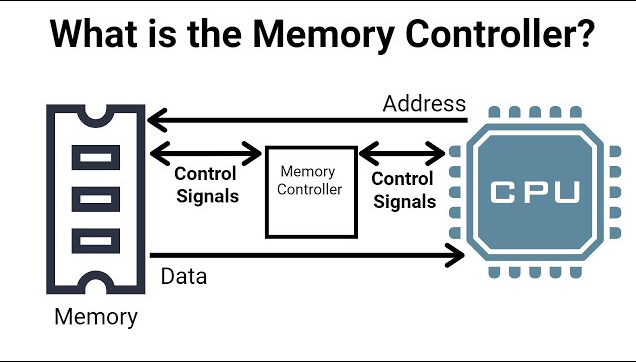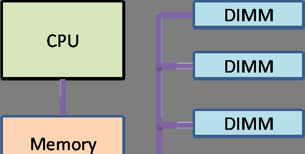
The memory controller plays a vital role in computer systems, overseeing memory operations and managing data flow between the memory and CPU. It sets the limits for maximum memory capacity, number of memory banks, type, speed, data depth, width, and other crucial parameters. This component significantly influences the computer’s memory performance, thereby impacting the overall system performance.

Categorization of the memory controller
Advancements in computer technology have led to the classification of memory controllers into conventional and integrated types.
In the realm of memory controllers, two primary categories exist: the traditional and integrated types.
Traditional Memory Controller:
In a conventional computer setup, the memory controller resides within the northbridge chip of the motherboard chipset. Data transmission between the CPU and memory involves a five-step process: “CPU-North Bridge-Memory-North Bridge-CPU.” This method, however, incorporates multi-level transmission, resulting in noticeable data delays that impact the overall performance of the computer system.
Integrated Memory Controller:
Contrastingly, an integrated memory controller is built directly onto the CPU. Consider a scenario without a memory controller: 26 data units, labeled A to Z, require transmission to the CPU. In this case, the CPU issues instructions to the northbridge. As the memory controller is integrated within the northbridge, data passes through it before reaching the memory. Addressing involves transferring these 26 data units, each sized at 500MB, to the CPU. Assuming a dual-channel R2 800 memory with a transfer rate of 12GB per second, the data reaches the CPU via the front-side bus (FSB) at a rate of 6.4GB per second, taking a total of 3 seconds for data transmission.
In contrast, within a CPU integrated memory controller system, the data travels from memory to the controller in 1 second, significantly reducing the transmission time. As the memory controller is at the CPU’s doorstep, data is directly read by the CPU. This efficient process optimizes CPU performance by swiftly accessing the 12GB of data in just 1 second, eliminating the need for the slower front-side bus.
To summarize: Without a memory controller, data transmission involves the memory controller, northbridge, and CPU. Conversely, with an integrated memory controller, the data path is simplified, directly from the memory controller to the CPU.
Working principle of the memory controller

Memory Frequency
Similar to the CPU, memory operates at its own frequency, measured in MHz. A higher memory frequency generally translates to faster memory performance within certain limits. The primary frequency of the memory module determines its maximum operational speed. Common memory types include DDR3 and DDR4. DDR3, succeeding DDR2, reached frequencies of up to 1600MHz, while DDR4 pushed further to 2133MHz.
Memory Capacity
Memory capacity not only influences memory pricing but also significantly impacts overall system performance. In the era of Windows XP, 512MB was standard, with 1GB considered ample. As 64-bit systems gained popularity with Windows Vista, 7, and 10, smooth operation typically required around 2GB of memory. Individual memory modules come in capacities of 1GB, 2GB, and 4GB, with higher limits reaching 8GB and 16GB.
Operating Voltage
Each type of memory operates optimally within specific voltage ranges, exceeding which could risk damaging the memory. DDR2 memory typically operates at around 1.8V, whereas DDR3 operates at approximately 1.5V or even 1.35V. Overclocking memory often necessitates higher-than-standard voltage settings, but this should stay within the manufacturer’s specified limits. While a slight voltage increase can aid overclocking, it generates more heat, posing a risk of hardware damage if not carefully managed within safe boundaries.
Timing Parameters
When delving into memory specifications, we often encounter timing parameters like “8-8-8-24,” which correspond to specific digital sequences, namely “CL-tRCD-tRP-tRAS.” The initial “8” represents the first parameter known as CAS Latency (CL).
CAS Latency Control, also referred to as tCL, CAS Timing Delay, or CAS Latency Time, governs the duration between receiving and executing an instruction. As it primarily manages the memory matrix’s column address or hexadecimal address, minimizing CAS latency is crucial for optimal performance while maintaining stability.
Memory access follows a sequence based on rows and columns. Upon triggering a request, it initially adheres to tRAS (Active to Precharge Delay). After precharging, the memory initializes RAS (Row Address Strobe) to address the required data. Beginning with the row address, followed by initializing tRCD, the cycle concludes by accessing the specific hexadecimal address through CAS. The period from the start to the end of CAS constitutes the CAS delay, signifying the final step in locating data and ranking as one of the most critical memory parameters.
This parameter regulates the number of clock cycles the memory waits post-data read instruction before execution. Simultaneously, it dictates the clock cycles needed for the initial phase of transfer in memory burst transfers. Smaller values optimize memory speed. However, some memory components may struggle at lower latency, potentially causing data loss. Conversely, increasing latency might enable higher-frequency memory operation. Therefore, when attempting memory overclocking, adjusting CAS latency can be beneficial.
Of all memory parameters, CAS holds the most substantial influence on memory performance. Lower CAS values, while ensuring system stability, enhance memory read and write operations, significantly impacting overall memory speed.
tRCD: RAS to CAS Delay
The second parameter in memory timing, as denoted in “8-8-8-24”, signifies RAS to CAS Delay (tRCD). This delay, also termed Active to CMD, refers to the time lapse between row and column addressing. A smaller tRCD value enhances performance by inserting a clock cycle delay between these addressing signals during memory reading, writing, or refreshing. Decreasing this delay can elevate system efficiency. For memory overclocking challenges, reverting to default memory settings or adjusting the tRCD value upwards might aid stability.
tRP: Row Precharge Timing
As the third parameter in “8-8-8-24”, Row Precharge Timing (tRP) denotes the time taken by the memory row address controller for precharging. A lower tRP accelerates memory read and write speeds by setting the duration for RAS to charge before activating another row.
tRAS: Min RAS Active Timing
Constituting the last parameter in “8-8-8-24”, Min RAS Active Time (tRAS) marks the briefest duration from an effective memory line to precharge. Adjusting this parameter typically falls within the 24~30 range, considering system-specific requirements. A longer tRAS cycle may impair performance by inducing unnecessary waits. Conversely, a shorter cycle might prematurely shift the activated row address to an inactive state, potentially disrupting data transmission. Ideally, this value aligns with CAS latency + tRCD + 2 clock cycles for optimal system performance and stability.
Advantage and disadvantage of the memory controller
Advantage of the memory controller
Integrating the memory controller within the CPU yields notable advantages. It enables efficient synchronization between the memory controller and the CPU core frequency. This direct link diminishes the need for data exchange through the northbridge, significantly reducing transmission delays. It’s akin to relocating a warehouse adjacent to a manufacturing workshop, slashing the time needed for raw material and finished product transportation. Consequently, this setup substantially enhances overall system performance.
Moreover, this integration alleviates the burden on the North Bridge chip. As CPU-memory data exchange constitutes a significant share of overall computer data transfer, integrating the memory controller eases the North Bridge’s workload. This, in turn, enables the North Bridge to offer more efficient support for data exchange channels like SATA, PCI-E, and others.
Disadvantage of the memory controller
Despite its merits, the integrated memory controller within the CPU does pose significant drawbacks. Its limited memory adaptability and flexibility constrain it to specific memory types, with restrictions on capacity and speed. Updating the CPU’s integrated memory controller to support new memory types necessitates replacing the entire CPU. For instance, AMD’s K8 series CPUs supported DDR but lacked compatibility with the faster DDR2. In contrast, traditional memory controllers located in the motherboard’s northbridge chip don’t encounter this issue. By replacing the motherboard alone, different memory types can be used without necessitating a new CPU. This flexibility was evident in CPUs like the Intel Pentium4 series, allowing users to switch between DDR and DDR2 simply by changing motherboards. Similarly, a motherboard supporting both DDR and DDR2 permits direct use of DDR2 without replacing the entire setup.
Conclusion of the memory controller
Numerous applications exhibit intricate read patterns, often approaching randomness, especially when unpredictable cache hits occur. Business processing software exemplifies such applications, where despite CPU enhancements like out-of-order execution, performance remains limited by memory latency. Consequently, the CPU awaits data retrieval before executing instructions, leading to inefficiencies. Even in low-end systems with memory latency around 120-150ns and CPUs operating at speeds exceeding 3GHz, a single memory request might squander 200-300 CPU cycles. Despite a 99% cache hit rate, the CPU might spend half its time waiting for memory requests to conclude, chiefly due to memory latency.
Traditionally, the memory controller in computer systems resides within the northbridge chip of the motherboard chipset. Data exchange between the CPU and memory occurs through a five-step process: “CPU-North Bridge-Memory-North Bridge-CPU.” This method involves multi-level data transmission, resulting in notable delays that hamper overall system performance. However, AMD’s K8 series CPUs, encompassing various processors utilizing Socket 754/939/940 interfaces, incorporate an integrated memory controller. This simplifies the CPU-memory interaction to just three steps: “CPU-memory-CPU,” omitting two steps present in the traditional method. This streamlined approach significantly reduces data delay compared to the conventional memory controller solution, contributing to enhanced overall system performance.


