Introduction of the Linear Regulator

In the preceding volume of this series, we provided a brief overview of the applications and placements of power management ICs in various domains. Within this page, our focus turns to exploring one particular form of voltage regulation known as the linear regulator.
Recall that voltage regulators come in two primary types: the linear variety and the switching variety. Among linear regulators, they can be further categorized into two distinct forms: the series type, which integrates a transistor as a variable resistor between the input and the load*1, and the shunt type, where a transistor is positioned parallel to the load. For the purpose of this discussion, we will exclusively delve into the series-type linear regulator, considering its broader usage compared to the relatively limited application of the shunt type. Let’s delve into the intricacies of the series-type linear regulator.
Linear Regulators
The most straightforward regulators, known as 3-pin regulators, deliver a consistent, fixed voltage output by incorporating an input capacitor (CIN) between the VIN and GND pins, and an output capacitor (COUT) between the VOUT and GND pins.
Now, let’s explore how these regulators achieve a stable fixed voltage output and discuss the components within linear regulators that facilitate this function. Below in Figure 1, we present an illustrative circuit structure of a linear regulator to detail its internal components and their role in maintaining a fixed voltage output.
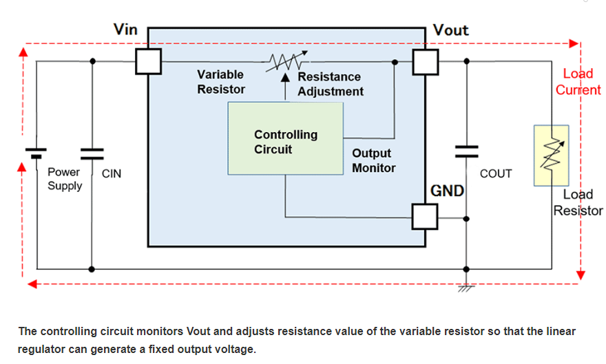
Internal Structure of Linear Regulator
The diagram demonstrates the supervisory role of the control circuit in monitoring the output voltage and adjusting the resistance value of the variable resistor. This adjustment enables the IC to consistently produce the predetermined fixed voltage. Specifically, when the input voltage (VIN) remains constant, a linear regulator achieves a steady output voltage by maintaining a fixed ratio between the variable resistance and the load resistance, adapting to any fluctuations in the load resistance value.
Linear regulators operate by dividing the input voltage using two resistors, resulting in an output voltage lower than the input. This discrepancy between the higher input voltage and the lower output voltage generates what’s known as waste heat. This heat arises from the difference between the input and output voltages. As the current flows through the load resistor, it subsequently passes through the variable resistor, where some of the electricity is consumed, generating heat in the process.
In Figure 2, these relationships are depicted. For instance, in a scenario where the load current is 100 mA, and the regulator functions with a 5 V input and a 2 V output, there’s a consumption of 0.3 W of electrical power (from the 0.5 W input) within the system, dissipating as heat.
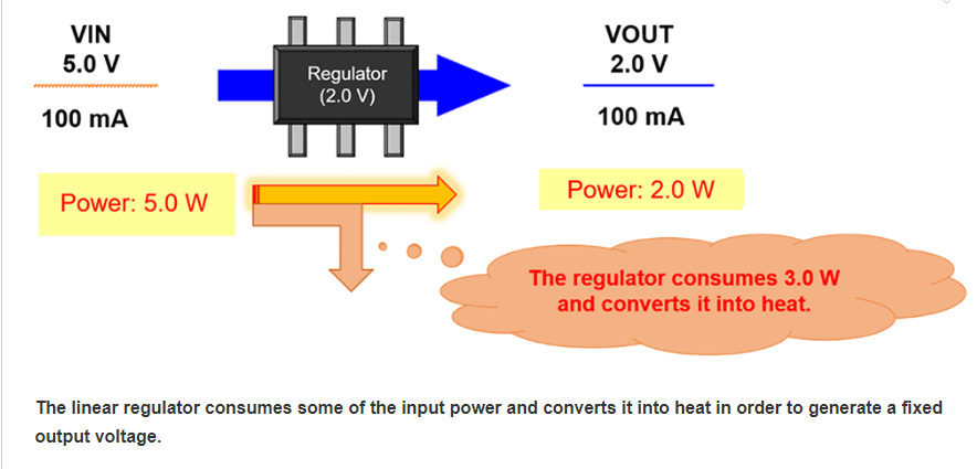
Circuit Structure of Linear Regulator
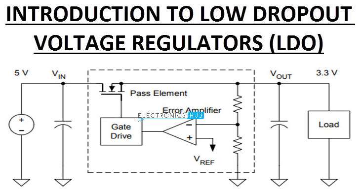
Linear regulators consist of four essential components: an output driver transistor, a reference voltage unit, a feedback resistor, and an error amplifier. Illustrated in Figure 3 is a rudimentary configuration representing the standard structure of a typical linear regulator.
Basic Structure of Linear Regulator
Output Driver Transistor: Figure 3 illustrates a linear regulator utilizing a MOS transistor as its primary component. This transistor essentially functions as the variable resistor depicted in Figure 1. In scenarios like the one shown in Figure 2, where both load and input currents amount to 100 mA, the VIN pin supplies the entirety of the current flowing through the driver transistor and subsequently to the load via the VOUT pin. To maintain a consistent output voltage, linear regulators modulate the resistance of the driver transistor with the aid of a control circuit (as depicted in Figure 1), which comprises a feedback resistor, a reference voltage unit, and an error amplifier.
Feedback Resistor: Often denoted as RFB, the feedback resistor plays a pivotal role in dividing the output voltage using two resistors (R1 and R2) and channeling this divided voltage back to an error amplifier. This divided voltage, termed as the feedback voltage (VFB), is instrumental in setting the fixed output voltage level of the linear regulator. The resistance ratio between R1 and R2 determines the output voltage level. Within specified ranges, the output voltage can be adjusted via laser trimming the resistance ratio of R1 and R2 in each wafer die during the manufacturing process. Some linear regulators offer a VFB pin, allowing users to connect an external feedback resistor to flexibly set the output voltage.
Reference Voltage Unit: Various methods are employed to construct a reference voltage unit, with most producing an output voltage level around 1 V. A common method involves a band gap reference (BGR) that utilizes the voltage difference between the base and emitter of a bipolar transistor, typically providing a 1.25V output voltage. Alternatively, CMOS-based reference units exploit the difference between the threshold voltage of two MOS transistors to generate a reference voltage ranging from about 0.6 to 1.0 V. Depicted in Figure 3 by a battery symbol, these units offer a smaller circuit size and extremely low supply current. Reference voltage units ensure a stable voltage level despite input voltage fluctuations or temperature changes, enabling linear regulators to produce a fixed output voltage.
Error Amplifier: Functioning as an operational amplifier, the error amplifier amplifies the voltage difference between its two input terminals—positive and negative—generating an amplified voltage output. Within a linear regulator, the positive terminal receives the feedback voltage, while the negative terminal obtains the reference voltage. The error amplifier processes the disparity between these voltages, amplifying the resultant voltage output, hence its name. This amplified voltage is then conveyed to the variable resistor. The interplay between these components within the negative feedback circuit of linear regulators ensures a constant output voltage by employing negative feedback control. This control mechanism compares the feedback voltage with the reference voltage, adjusting the resistance of the output driver transistor to nullify the difference.
Operation of Linear Regulators
Let’s explore the internal operation of a linear regulator as outlined in Figure 4, focusing on how it responds when the load resistance undergoes changes. When the load resistance diminishes and the load current surges, both the output voltage and the feedback voltage decrease simultaneously. Consequently, the output voltage from the error amplifier declines as the feedback voltage falls below the reference voltage. This reduction prompts a decrease in the driver On-resistance. As the load current increases, this reduction in the output driver On-resistance aids in restoring the output voltage to its predetermined value. Once the output voltage reaches its set value, the feedback voltage aligns with the reference voltage.
Conversely, a decrease in the load current elevates the output voltage of the error amplifier and the driver On-resistance. This elevation occurs due to the heightened output and feedback voltages resulting from the decrease in load current. The rise in the driver On-resistance, correlated with the decrease in load current, facilitates the return of the output voltage to its designated value.
LDO Regulators
By the way, there’s a subgroup of linear regulators known as LDO regulators, where LDO stands for Low DropOut. But what does ‘low dropout’ actually mean? Dropout voltage (VDIF) is a specification for linear regulators, indicating the minimum difference required between input and output voltages for the regulator to maintain a set output voltage within an acceptable range*3. If the difference between input and output voltages falls below this dropout voltage, the linear regulator fails to sustain the set output voltage, causing a drop in output.
Consider a scenario where a linear regulator draws power from a battery. For the regulator to maintain a stable output voltage, the input voltage should exceed the sum of the desired output voltage and the dropout voltage. Consequently, the lower the dropout voltage of the linear regulator, the longer the battery can operate.
Now, let’s examine a linear regulator powered by a DC/DC converter. If the DC/DC converter is set to output a voltage slightly higher than the combined value of the output voltage and the dropout voltage of the linear regulator, it can ensure stable operation. In such cases, using a regulator with a lower dropout voltage significantly reduces power loss compared to one with a higher dropout voltage. For instance, a regulator with a 0.2 V dropout voltage can halve power loss when compared to a regulator with a 0.4 V dropout voltage. However, it’s crucial to note that merely swapping to a regulator with a lower dropout voltage won’t reduce power loss unless the set output voltage of the DC/DC converter is adjusted accordingly.
This advantage distinguishes regulators with low dropout voltages, often termed LDO regulators. However, it’s essential to mention that there’s no standardized definition for LDOs, leading to variations in interpretation among different companies. As a result, the term LDO is frequently used as a concise reference for any type of linear regulator in many instances.
Dropout Voltage and Output Current
Dropout voltage is determined under specific output conditions. For instance, in Figure 6, the dropout voltage is depicted with an output current of 150 mA. As previously mentioned, the driver transistor functions as a variable resistor. Considering this, let’s explore the relationship between dropout voltage and output current using Ohm’s law, treating the driver as a resistor.
In this case, the minimum dropout voltage measures 0.23 V, occurring at an output current of 0.15A. Calculating the driver resistance using Ohm’s law yields:
This calculation indicates the minimum driver resistance of the LDO regulator.
Now, based on this resistance value, let’s compute the permissible output current for a 0.1 V difference between input and output voltages.
The computation suggests that to maintain a 3.0 V output at a 3.1 V input, the output current of this LDO regulator must remain below 65 mA. Consequently, if this LDO regulator outputs 150 mA at a 3.1 V input, the resulting output voltage would be 2.87 V. This situation would cause the output voltage to drop 0.23 V below the input voltage and 0.13 V below the designated output voltage.
Based on the earlier calculation, introducing a second driver transistor in parallel could enable this LDO regulator to produce 150 mA at 3.1 V by halving the driver’s on-resistance and doubling the output current. Yet, Picture 8, displaying the circuit of the LDO regulator, highlights that a substantial portion of the chip area is already occupied by the driver.
Expanding the output current or reducing the dropout voltage necessitates decreasing resistance, a task achievable by integrating two driver transistors in parallel within this confined space. However, this enhancement requires doubling the driver area and consequently enlarging the chip area, leading to an increase in manufacturing costs. Balancing regulator specifications with cost considerations becomes crucial in this context.
Conclusion
Throughout this session, we’ve delved into the inner workings of a linear regulator, elucidating how it maintains a steadfast output voltage despite fluctuations in input voltage or load current. In essence, a linear regulator achieves this feat by constantly monitoring the output voltage and employing a negative feedback circuit to fine-tune the internal driver’s on-resistance. This mechanism ensures the linear regulator can sustain a stable voltage output, even when fluctuations in input voltage or load current create disparities between the output voltage and the predefined voltage setting.
Additionally, we’ve introduced several specifications that delineate the output stability of a linear regulator, such as input regulation, load regulation, and the critical dropout voltage, essential for upholding a consistent output voltage. Notably, these specifications are unaffected by time variations.
Moving forward, our focus will shift to elucidating time-dependent specifications. We’ll explore the limitations of power dissipation crucial for maintaining the stable operation of linear regulators. Furthermore, we’ll unravel the roles played by input and output capacitors, shedding light on their significance in the functionality of these regulators.


